Layout
|
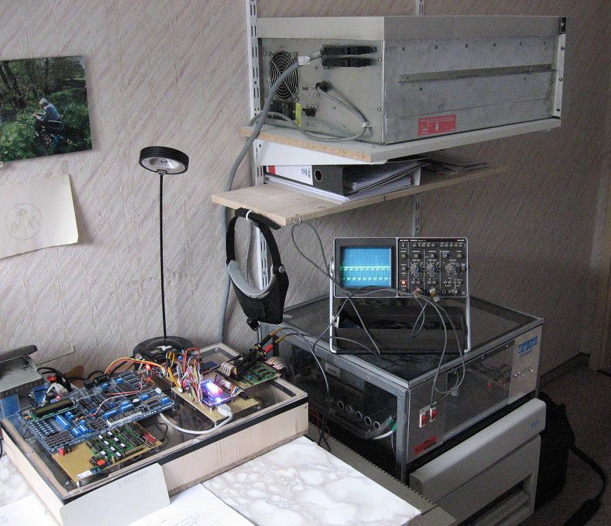
My current development environment in my study is visible in the following picture. The RL02 disk drive was screwed for place reasons to the wall. After all almost 40 kg heavy. Under the RL02 disk drive the Scope and my PDP-11/23 SE (chapter 5) can be recognized. In this picture the Micro-PDP 11 cannot be seen which is located between desk and PDP-11/23s SE. The simulator hardware can be recognized on the desk. |
The most important specifications of the RL02 disk drive
|
Physical Specification |
19 inch RETMA Rack compatible Depth: 63.5 cm , Height: 26.5 cm Weight: 34 kg ( emty ) |
|
Generel |
Linear bit density: 147 Bits/mm Number of sectors: 30/track Number of recording tracks: 512/surface, Number of Surface:2 Encoding method: MFM |
|
Transfer Rate |
4.1 magabits/sec +/- 1% , Bit Cell With: 244 nsec , Words(16 bit): 256 kilowiords/sec +/- 1% |
|
Seek Time |
Average: 55 msec ( 120 tracks ) One cylinder track 4 msec max seek time. |
More RL02 specific information : RL02-Documentation
|
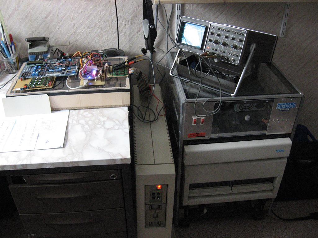
Here another picture from another viewpoint with visible Micro-PDP 11. |
Start
|
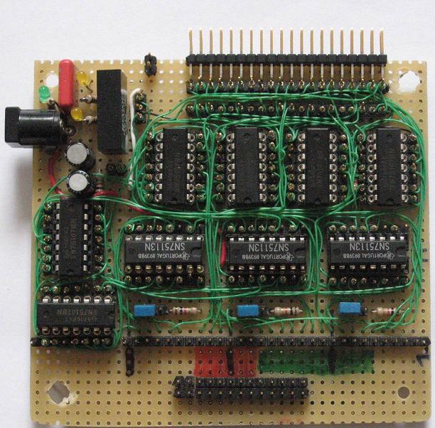
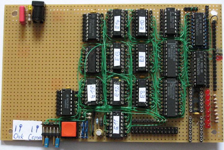
The construction started in September 2009. First, a possibility had to be found to measure the differential RL02-bus signals and convert it to TTL level for further processing . For this purpose I designed a special, 40-pole ribbon cable for the connection between RLV-12 controller and the RL02 disk drive. Therefore I was able to watch the RL02 bus signals. The RL02 bus architecture is based on +5V/-5V differential signals, 6 signals each for the two directions. I didn't find any substitute for the necessary bus Receiver/Transmitter chips and had much trouble to get the original chips of the type 75113 and 7510. In the end after many searches I was successful anyway and the chips could be obtained via the dealer sh-Halbleiter in Germany. The board is designed in Wire-Wrap technology like in the following picture, based on the circuit diagram from the RLV-12-engineering-drawings . To get the required DC power, +5V/-5V, an additional DC/DC-Converter was installed. To be able to watch and check the transmitter read signals from the drive to the controller, I installed 3 additional 7510 receiver chips. The 40-Pin Connector of the RL02 bus is visible in the upper part of this picture. |
|
|
|
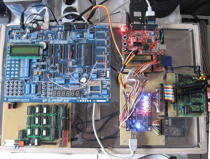
A) In the summary the complete development hardware can be seen here. The QL200 PIC MCU Development board is above on the left visibly. It was the first attempt and it turned out very fast, though, that a PIC 16 bit MCU was completely insufficient for this project. Programming based on assembler language with the Integrated Development environment MPLAP of MICROCHIP wasn't a problem for me and it turned out very fast that the throughput and the frequency range didn't suffice with 8 bits. Bad investment for this project at this point in time, but it went on ... |
|
|
|
... and here are all 3 actively connected components visible ( FEB 2010): |
|
|
|
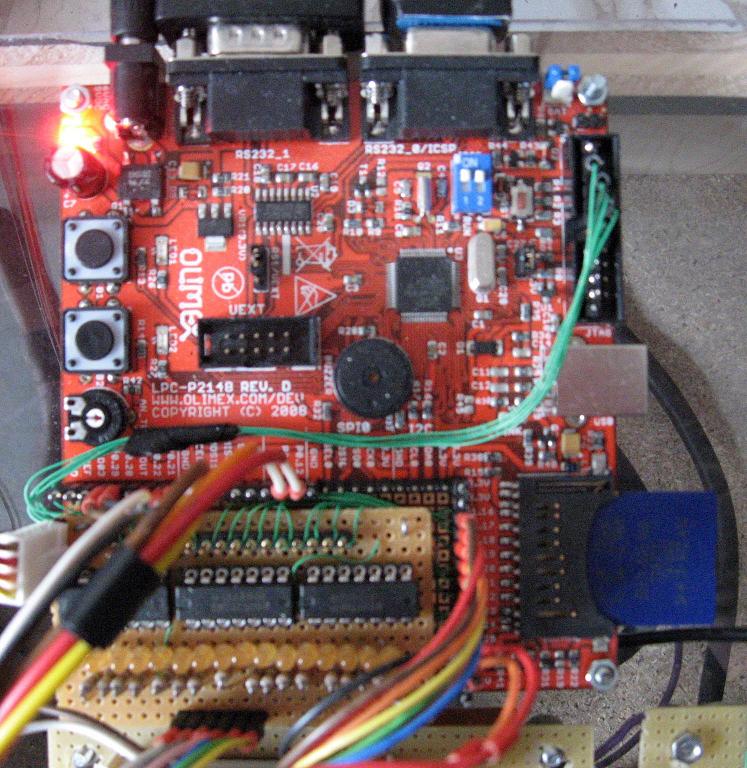
B) I was in the decision phase in October 2009, which MCU is suited best for this project. After investigating for a long time I have decided in favor of the LPC-P2148 Development board of OLIMEX. This board works with a MCU: 16/32 bit ARM7TDMI-S™ ( Fa. Philips ) with 512K Bytes Program Flash, 42K Bytes RAM, USB 2.0, RTC, 10 bit ADC 2.44 uS, 2x UARTs, 2x I2C, SPI, 2x 32bit TIMERS, 6x PWM, 8x CCR, 1x DAC, WDT, 5V tolerant I/O, up to 60MHz operation. This board was ideally suitable for the getting in and very well for the developmental stage. This board isn't the final version, though and will then replaced by another like such as LPC-H2294 . This will become necessary because a SD card only can handle a restricted number of write cycles. The final version will hold the RL02 data in RAM and the SD-Card will be used just for the load and store operations. In the following picture my LPC-P2148 board can be seen with additional 16 LED's to be able to watch the 16 bit based data transfer visually. |
|
|
|
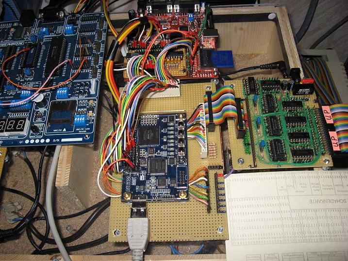
C) It went on rather toughly now. The setup of the software development environment had to be implemented (see 1.4) and the hardware of the RL02 Simulator had to be developed step by step. The base for this project is to be able to read the RL02 drive command register. In the first step I therefore developed a circuit diagram to read the command register of the RL02 disk drive. Since I was still an engineer of the old style I built the design based on TTL-Chips and Wire-Wrap technology. It wasn't simple for me but I managed to complete this board and I was able now to read the RL02 Drive-Command-Register. The circuit diagram to this is open here: Drive-Command-Register |
|
|
|
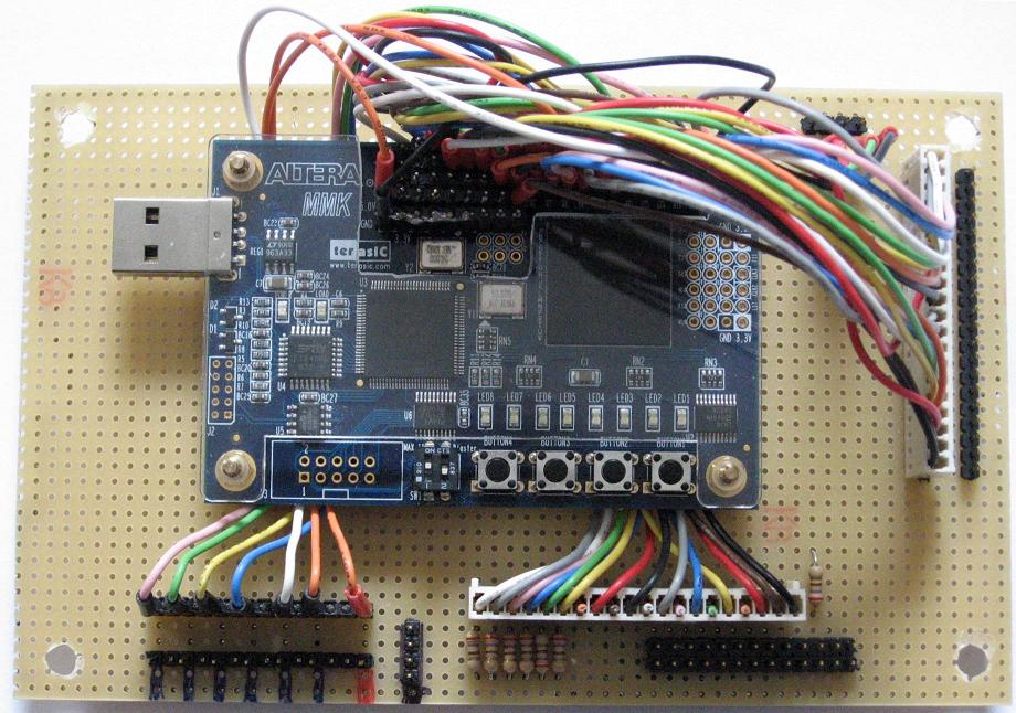
D) The greatest breakthrough at this project was: FPGA ( Field Programmable Gate Array ). Myself, also already an “OLDIE“ refused this new technology to employ me very long and I am annoyed afterward because I hadn't made this step earlier. I had arrived in the embedded systems world and it was going on speedily now. I decided in favor of the MAXII-FPGA of ALTERA. To make the start in the FPGA-world as simple as possible I bought the Development board , MAXII-Micro-Kit-Board , at Digi-Key, manufactured by Terasic-Technologies-Inc . This board is ready for use, includes the MAXII FPGA and also a USB Blaster for downloading the compiled circuit diagrams. With the enclosed Quartus II web edition software of ALTERA, I was able to develop a circuit diagram into a fraction of time. The Micro-Kit-Board has been built up pin-compatible to the above TTL-design like in the following picture obvious. |
|
|
Résumé:
I
need soldering no more and threading Wire-Wrap